
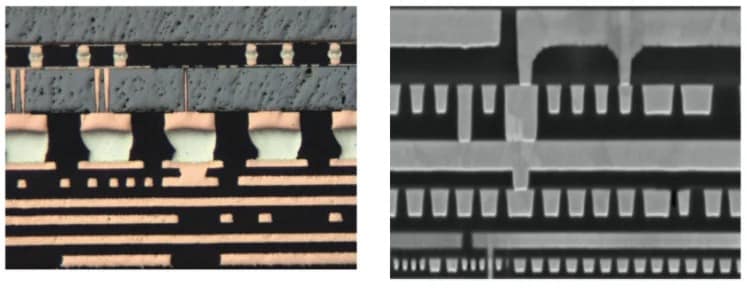
HENSOLDT announced this week that using the newly developed dielectric polymer and Nano Dimension’s conductive ink, the company has successfully assembled the first 10-layer printed circuit board (PCB) and mounted its electronic components on both sides of the board.
This is the first time that a 3D printed board can withstand the difficult soldering process required for a double-sided board.
The Possibility of additive manufacturing and 3D printing
Building a multilayer PCB is an expensive and time-consuming prospect. However, until the manufacturer produces such a board, the product is a dream, and only exists in the storage unit of the simulator. What is needed is a fast and inexpensive method to come up with real physical prototypes.
A complex board can be generated at a relatively low cost (one day instead of several weeks). In the development phase, there is nothing more frustrating than putting the panels together to reflect the revised design.
Achieving rapid turnaround through additive manufacturing can quickly provide the latest circuit boards. In addition, for products produced in small batches, PC printing can meet the requirements of the entire product cycle, and engineering changes can be easily made, thereby greatly reducing time and saving money for rapidly developing equipment.
Finally, additive manufacturing can greatly help impedance control, which requires precise manufacturing of PCB interconnects.
As described in Nano Dimensions, using 3D printing for PCB manufacturing allows designers to go beyond the standard trace geometries available in standard planar manufacturing processes, thereby ensuring strict impedance control.
Long-term partnership between HENSOLDT and Nano Dimension
HENSOLDT has been using Nano Dimension’s Dragonfly technology for 3D printing.
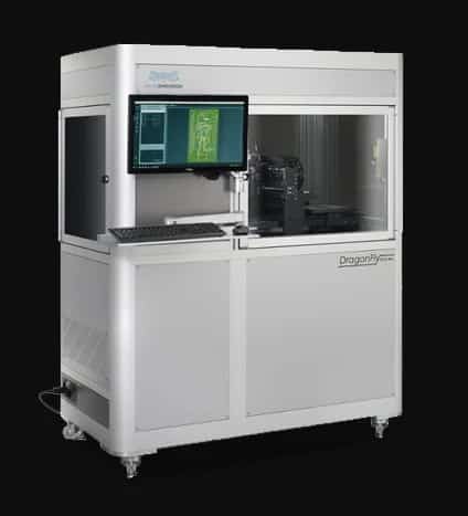
This additive manufacturing platform integrates the inkjet deposition printer with its own nano-ink and 3D software. This machine can print electronic circuits such as antennas, capacitors, PCBs and sensors.
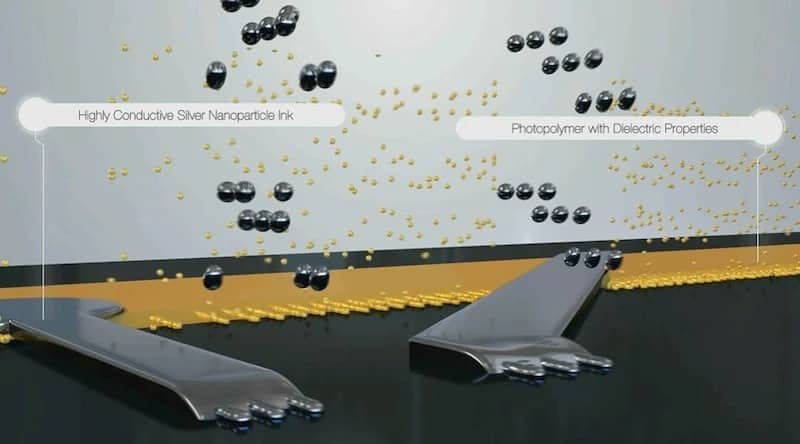
The dual printhead structure allows DragonFly LDM to print with both dielectric polymer ink and conductive ink in a single print job, which reduces the time to completion.
3D manufacturing: best for prototype design and short-term production
Manufacturers like HENSOLDT can take advantage of additive manufacturing to gain huge advantages. Thomas Müller, CEO of HENSOLDT, explained: “The performance and reliability requirements of military sensor solutions are much higher than commercial components. High-density components are quickly provided by 3D printing in a labor-saving manner, which allows us to Has a competitive advantage in the development process. ”
Although many observers mistakenly regard 3D manufacturing as a way to produce simple products in large quantities, the real future of the technology seems to lie in prototypes and short-term equipment. For manufacturers like HENSOLDT that require the most stringent control, the technology may change the rules of the game.